SHMZ MEMS-Casting Semiconductor Technology Co., Ltd.
The main personnel of the R&D team are from the Institute of Microsystems and Information Technology of the Chinese Academy of Sciences.
The company is committed to the development and industrialization of wafer-level liquid alloy micro-casting technology, the main application areas are semiconductor advanced packaging, MEMS devices and three-dimensional integrated passive devices.
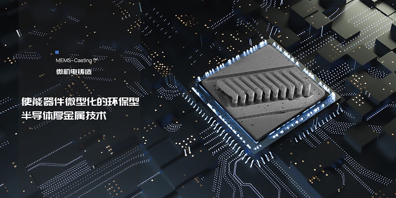
MEMS-Casting
MEMS-Casting is composed of two words, MEMS and Casting. MEMS is the acronym for English Micro-Electronic-Mechnical System, which is a proper noun. MEMS is an industrial technology that integrates microelectronics and mechanical engineering. Its operating range is in the micrometer range (generally several micrometers to hundreds of micrometers). The processing technology of MEMS is transformed from semiconductor processing technology and can be considered as a branch of integrated circuit manufacturing technology. The difference is that integrated circuits manufacture logic operation circuits on wafers, while MEMS manufacture micromechanical structures on wafers, such as cantilever beams, comb-like structures, and cavity thin film structures. MEMS is the main processing and manufacturing technology for chip sensors. Casting is English for casting. MEMS-Casting is the casting in the field of micro-electro-mechanics, which can be referred to as micro-electro-mechanical casting for short. MEMS-Casting is a micro-scale casting realized on a wafer. It is so named because this micro-casting technology is based on MEMS technology and is used in the MEMS field in many ways.

MEMS-Casting is a multidisciplinary fusion technology
MEMS itself is a multidisciplinary technology. MEMS-Casting is a wafer-level manufacturing technology developed by integrating fluid mechanics, thermodynamics, metal science, casting, mechanical engineering, electrical engineering and semiconductor-related technologies in physics. . From technical principles, equipment prototypes, process flow to device realization, MEMS-Casting technology completes a systematic research and development process, and is also a case of technological achievement transformation from the laboratory to the production line.
MEMS-Casting is a semiconductor thick metal technology
Metal structure is an important part of semiconductor devices. There are currently three main metal processes in semiconductors: physical vapor deposition (that is, evaporation or sputtering), chemical vapor deposition and electroplating, as shown in the following table. Among them, PVD and CVD are generally only used for the deposition of thin metals (thickness less than 1um) because of their slow deposition speed. For thick metal deposition technology, electroplating was the only method before. MEMS-Casting provides the industry with a new method of thick metal deposition.
The main technology of semiconductor metallization (Metallization)
MEMS-Casting is an alternative and supplement to electroplating
MEMS-Casting can be used as an alternative and supplement to electroplating. Compared with electroplating, MEMS-Casting has the advantages of simpler process, faster deposition speed and clean and environmentally friendly process.
success case
Via interconnect filling for semiconductor advanced packaging
specifications:
Substrate: silicon/glass/ceramic
Wafer size: small piece/4”/6” (8” equipment under development)
Aperture: depth/diameter respectively >20um
Pass type: through hole/blind hole
CMP required: Yes
Alloy material: zinc aluminum alloy/melting point 380 degrees/conductivity of 6.5μΩ.cm (approximately 25% copper)
Process temperature: ~425 degrees
MEMS SOLENOIDS WITH MAGNETIC CAVITY
MEMS spiral coil
Successfully developed a miniature U-shaped electromagnet. This electromagnet is smaller than a fingertip and aims to become the smallest U-shaped electromagnet in the world at this stage. Compared with a straight spiral coil, a U-shaped coil can form a closed magnetic circuit, and the electromagnetic force generated as an electromagnet can be dozens of times larger than that of a straight electromagnet. However, the structure of the micro U-shaped coil is much more complicated than that of the straight coil, and it is difficult to achieve miniaturization by using the traditional enameled wire winding method. The MEMS-Casting technology can perfectly solve this problem, and can achieve mass manufacturing.
μCasting™ Solenoid coil is a chip-level spiral coil manufactured based on MEMS bulk silicon etching process and MEMS-Casting™ technology. μCasting™ Solenoid belongs to the next generation of microchip coils.
specifications:
Number of turns: 5~200 turns
Line width: >20 microns
Line spacing: >20 microns
RF DEVICE
MEMS-Casting technology can be used in the manufacture of radio frequency devices. Such as chip type micro coaxial cable, distributed filter, etc.
Fanout
MEMS-Casting is used to manufacture complex three-dimensional Fanout structures

